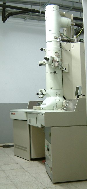
Transmission Electron Microscope

NAME | TEM |
|---|---|
| Transmission Electron Microscope | |
Function | 1. Penetrating image observation (up to nm level) 2. Electron diffraction for crystal structure analysis (available for SAD and NBD). 3. Provide high-brightness electron beam with spatial resolution, suitable for diversified test piece analysis. |
Purchase Date | 93.07.30 |
Purchase Amount | NT 7,595,095 |
Label | JEOL |
Model | JEM2010 |
Instrument Specifications | 1.Performance: ●Resolution:0.25nm(point resolution)、0.14nm(Lattice Resolution) ●Magnification:50 to 1200000x 2.Electron Optics: ●Electron gun: LaB6 ●Energy spread (eV): 1.5 ●Condition Lift (hr):10000 ●Vacuum (Pa):10-5 ●Temperature (K):1800 ●Short time stability: 1% ●long time stability:3% Hr ●Current efficiency:100% 3.TEM mode: Image observation, the resolution can reach 0.23nm (AHR), the magnification can reach more than one million, and the OBJ aperture can be used to observe bright field images (Bright field image, general observation) or dark field images (Dark field image, a specific diffraction crystal plane or defect observation). 4. SAD mode: Selected area diffraction uses selected area aperture to do um-level diffraction to identify the crystal structure. 5. NBD mode: Micro-area diffraction (nano beam diffraction) uses a fine electron beam for nm-level diffraction to identify the micro-area crystal structure. 6. Digital CCD imaging system: ●CCD Active area: 36mm × 24mm ●CCD Size: 4008 × 2672 pixels, each pixel 9μm × 9μm |
Additional accessories | 1.Single Tilting Holder: Standard sample holder 2.Double Tilting Holder: Beryllium material, double tilting base: X-axis ±40°±; Y-axis ±30°. 3.Cooling Double Tilting Holder: Applicable to materials or biological samples that are easily damaged by heat. |
