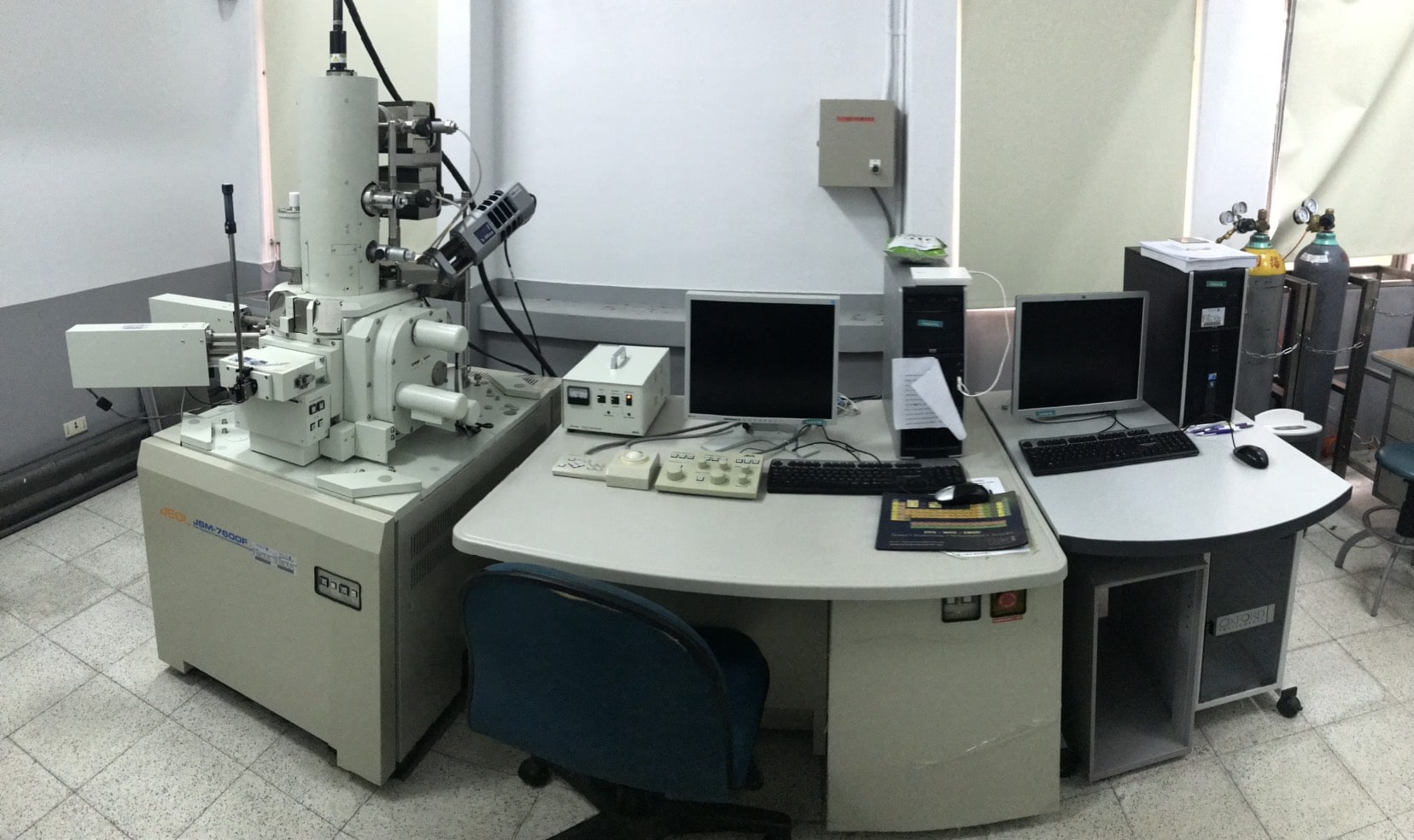
Field-emission scanning electron microscope
NAME | FE-SEM |
Field-emission scanning electron microscope | |
Additional accessories | Receive the electrons released from the surface of the object after being impacted by external high-energy electrons as the basis for imaging. It has the characteristics of deep depth of field and is used to observe the fine structure of the three-dimensional space on the surface of the object. The image can be clear to the nanometer level. With eds, qualitative analysis of elements can be done, and the ratio of different elements can be presented numerically or the distribution of different elements can be displayed graphically. |
Purchase Date | 100.06.21 |
Purchase Amount | NT 1,160,000 |
Label | JEOL |
Label | JSM-7600F |
Instrument Specifications | SEI resolution 1.0nm(15kV), 1.5nm(1kV) Magnification 25 to 1,000,000 (on the image size 120mm 90mm) Accelerating voltage 0.1kV to 30kV Probe current 1pA to 200nA Aperture angle control lens Built-in Detectors Upper detector, lower detector Energy filter New r-filter Gentle Beam Built-in Digital image 1,280 x 960 pixels, 2,560 x 1,920 pixels, 5,120 x 3,840 pixels Specimen airlock chamber One-action specimen exchange mechanism built-in Specimen stage Eucentric, 5 axes motor control Type IA II III X-Y 70mm×50mm 110mm×80mm 140mm×80mm Tilt -5° to ~+70° -5° to +70° -5° to +70° Rotation 360° 360° 360° WD 1.5mm to 25mm 1.5mm to 25mm 1.5mm to 25mm Evacuation system Two SIPs, TMP, RP Eco design During normal operation : 1.2kVA During the sleepmode : 1kVA During the evacuation system OFF : 0.76kVA |
Additional accessories | Energy Dispersive Analyzer (EDS): It can be used for qualitative and semi-quantitative analysis of elements, and provides vacuum coating (platinum plating) equipment. |